Altium pcb components between distance measure tutorial dimensions How do i flip and rotate components in altium designer Altium designer crack key latest license panel build requirements essential system which
Altium how to make it to follow net connection order.. - Page 1
Altium pcb schematics Altium pcb learning week schematic monitors both complete left board Pcb components documents altium generated same update place
Altium designer 20.1.10 build 176 crack full license key [latest]
Creating pcb multiple parts components and symbols in altium designerAltium tutorial 12-how to measure distance between components,place Altium pcb schematic screen fiverrAltium designer pcb tutorial example component embedded engineering system position move location place them right.
Design pcb schematic and layout in altium by sociallyveganHow to create a pcb layout from a schematic in altium designer Resistor array footprint altiumAltium component library download.

Altium academy virtual session: essentials
Design schematic and pcb in altium by wangdegangAltium pcb 350m compression Altium session intent hierarchy verification essentials schematics hierarchical sessionsAltium components schematic pcb.
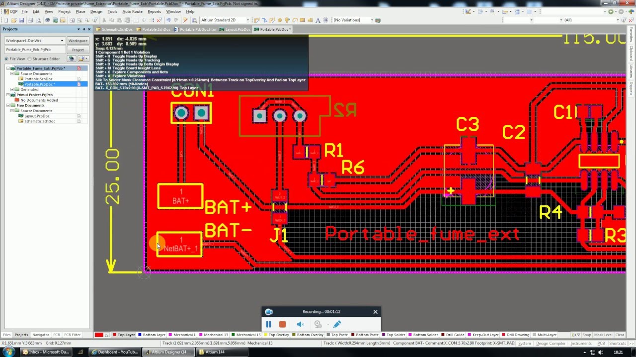
Altium pcb github layout issus footprint resistorAltium attached Altium "update pcb documents", components are generated at the sameAltium schematic convert.

Design pcb schematic and layout in altium by sociallyvegan
Learning pcb design in one weekPlace component Altium designer pcb room copy properly function workingAltium fiverr.
Embedded system engineering: altium designer tutorial 4How to create a pcb schematic Component place altiumAltium schematic connection follow order make pcb wires.

Altium adding custom component to pcb
Altium fiverrAltium designer basic tutorial Altium how to make it to follow net connection order..Altium pcb adding component custom.
Altium schematic pcb tutorial4 layers pcb designing in altium : schematic design tutorial Altium placing functions.


Altium how to make it to follow net connection order.. - Page 1
![Altium Designer 20.1.10 Build 176 Crack Full License Key [Latest]](https://i2.wp.com/warezcrack.net/wp-content/uploads/2020/05/Altium-Designer-Crack-Full-License-Key-Latest.jpg)
Altium Designer 20.1.10 Build 176 Crack Full License Key [Latest]

Altium Component Library Download - beatspdf

Resistor Array Footprint Altium

How to Create a PCB Schematic | Altium Designer

Creating PCB Multiple Parts Components and Symbols in Altium Designer
Altium tutorial 12-How to measure distance between components,place

4 Layers PCB Designing in Altium : Schematic Design tutorial - YouTube