41 change pcb board size in altium designer 18 Layout guide to changing board sizes in altium designer Altium designer
Layout Guide to Changing Board Sizes in Altium Designer | PCB Design
Altium board designer pcb changing sizes layout setting origin default set Altium board designer changing sizes cutout pcb adding Altium pcb designer: get size from sheet layer
Altium tutorial-21: how to print exact size layout layers
How to choose a pcb board sizeAltium board guide changing sizes layout designer Altium circuitmaker – paxspace, incStandard pcb panel size-what you need to know.
Altium pcb dimensionsAltium sheet top duplicate names nets Set pcb size with values altiumAltium pcb component designer height thermal.

Altium designer pcb design tutorial
Altium print exact layoutLayer pcb altium mechanical assign Altium pcb designer: get size from sheet layerEmbedded system engineering: altium designer tutorial 4.
Altium designer pcb tutorial example component embedded engineering system position move location place them rightPcb board size choose circuit Pcb altium tutorial designer string add clickPerfect styling for your organisation with altium 365.

Altium schematic connection follow order make pcb wires
Pcb altium board size wizard values set define shape using another need way stackAltium pcb Altium how to make it to follow net connection order..Pcb design.
Layout guide to changing board sizes in altium designerPcb altium dimensions information thru opened reports menu which board stack Altium properties selectLayout guide to changing board sizes in altium designer.

Pcb altium circuitmaker wizard eagle kicad geda compete existing designspark windows
.
.


pcb design - Altium duplicate net names on top sheet - Electrical

Embedded System Engineering: Altium Designer Tutorial 4 - PCB Layout

Perfect Styling for Your Organisation with Altium 365 | Altium PCB

Layout Guide to Changing Board Sizes in Altium Designer | PCB Design

41 Change PCB board size in Altium designer 18 - YouTube

pcb - Component Height - Altium Designer - Electrical Engineering Stack
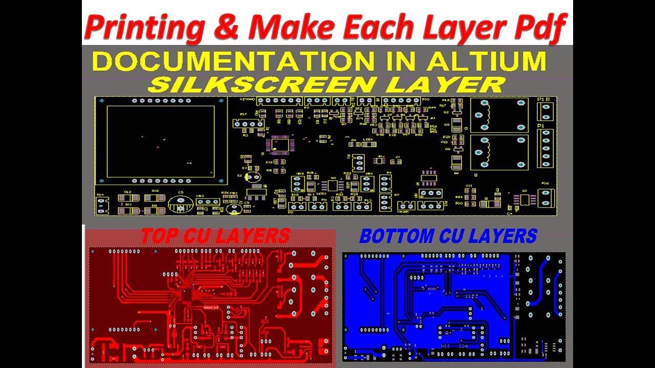
ALTIUM TUTORIAL-21: How To Print Exact Size Layout Layers

Altium PCB dimensions - Electrical Engineering Stack Exchange